Doping Silicon with Lasers


Breaking Taps
@breakingtapsAbout
Exploring material science and machining For Youtube business, sponsorships, etc: [email protected] Optical Microscopes: - Amscope 40X-800X Trinocular Dual-illumination Metallurgical Microscope with Polarization - Amscope 3.5X-180X Simul-Focal Stereo Zoom Microscope Atomic Force Microscope: - ICSPI nGauge AFM (100nm wedge tips and 20nm DLC tips) Scanning Electron Microscope: - Thermo Phenom XL G2 (BSD, SED and EDS)
Latest Posts


Video Description
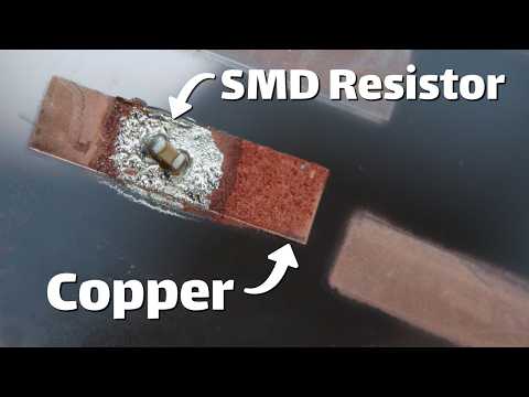
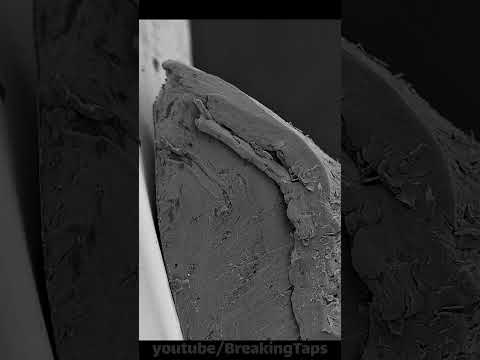
Today we're doping silicon wafers with a phosphoric acid and a fiber laser. CONSIDER SUBSCRIBING 🥰 ☕Buy me a coffee? https://www.buymeacoffee.com/Breakingtaps 🔬Or Patreon if that's your jam: https://www.patreon.com/breakingtaps 📢Twitter: https://twitter.com/BreakingTaps 💻Discord: https://discord.gg/R45uCXcEv4 ==== Details ==== Impurity dopants are traditionally introduced into a wafer via thermal diffusion, or ion implant. There is an alternate method using lasers to drive the dopant into the wafer, a sort of targeted thermal diffusion. This technique is used in the solar panel industry to form back contacts and selective emitters. The laser selectively vaporizes the phosphoric acid and melts the silicon, allowing phosphorus to diffuse into the molten region. After the laser pulse ends, the silicon resolidifies and the impurity is trapped inside. Sam's video on RIE: https://www.youtube.com/watch?v=RoQgnC0Oz2k ==== Analysis Equipment ==== nGauge AFM from ICSPI (https://www.icspicorp.com/) Phenom XL SEM from Thermo Gwyddion for AFM post-processing Blender for 3D AFM rendering ==== Timeline ==== 0:00 Intro 0:39 I have no idea what I'm doing 1:09 Doping silicon 2:21 Thermal diffusion 3:19 Ion implantation 4:36 Laser doping 10:06 Resistivity test 10:40 Hot probe test 12:20 Diode test? 15:57 SEM Archive 17:06 Next steps 17:26 New hat!
You May Also Like


Upgrade Your Silicon Doping Setup
AI-recommended products based on this video

Portable 2-Wheel Oxygen Cylinder Cart, 23.5cm Diameter Oxygen Tank Trolley with Handle, Rolling Gas Bottle Storage Rack for Home Use, Lightweight Oxygen Tank Transporter

Rolling Oxygen Tank Holder Cart with 2 Wheels, Handle & Safety Belt - Portable Oxygen Cylinder Trolley & Storage Rack for Home Use, Fits 23.5cm Gas Bottles
