Why Ground Planes Can Break RF... And How to Fix It


Hans Rosenberg
@hansrosenberg74About
No channel description available.
Latest Posts


Video Description
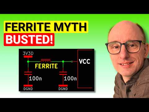
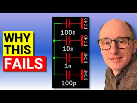
Free mini-course: https://www.hans-rosenberg.com/minicourse_account_youtube?utm_source=yt-d-v4 Full course info: https://www.hans-rosenberg.com/epdc_information_yt?utm_source=yt-d-v4 Other videos - https://www.youtube.com/watch?v=EEb_0dja8tE&list=PLsWHPs7La-3KUY2JDUyrz0Jc0xw8kH4zQ In this series, I'm going to show you some very simple rules to achieve the highest performance from your radio frequency PCB design for your electronics project. I'll do this by showing you how to improve the grounding and reduce the crosstalk. These rules apply to both analog , digital and RF electronics. I'll also share some rules of thumb for PCB parasitics that you can use in electronics simulations. I'll prove my points with actual measurements on dedicated test PCBs. In this fourth part I'm showing the advantages of ground on all layers, and how to get rid of the potential disadvantages. Website: www.hans-rosenberg.com 00:00 Introduction 00:19 What is ground on all layers? 00:44 pros and cons of ground on all layers 01:46 Copper balance explained 02:25 The measurement setup 03:39 measurement results 04:38 measurement result analysis and calculations 06:31 Conclusions 07:16 Via layout strategy 08:00 Thank you and unexpected end screen
You May Also Like


PCB Design Essentials
AI-recommended products based on this video

5.0 Upgraded Magnifying Glass Hand Free【12X German Ultra-HD Lens】【Cloud Sponge Neck Protection】 3 Smart Mode Light, All-Purpose Magnifying for Reading, Cross Stitch, Craft Seniors Use (Black)

GULINEE Wet and Dry Cut Professional Hair Cutting Scissors Barber Shears Japanese Aichi SUS440C Stainless Steel Tijeras de Peluqueria Shintou (5.5" Precision Cut)

Digital Multimeter Voltmeter Battery Voltage Multi Tester AC DC Volt OHM Amp Current Meter Circuit Continuity Resistance Diode Electrical Tester with Test Leads Backlight LCD Display
